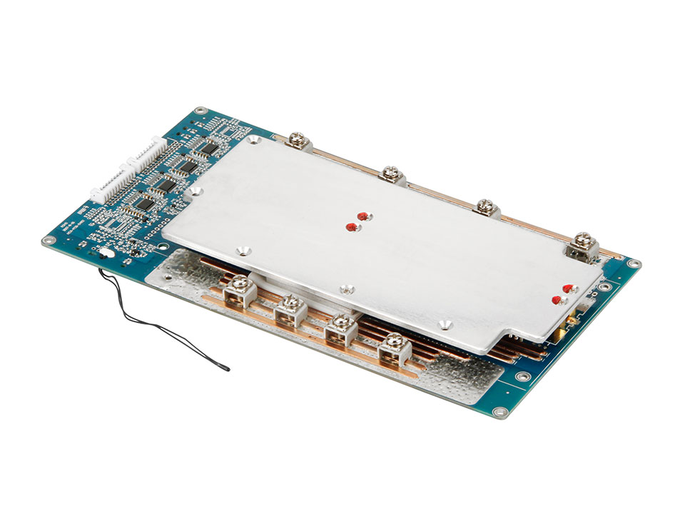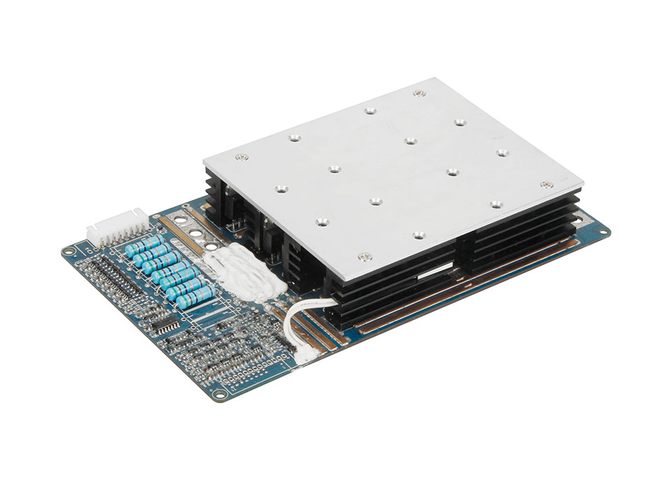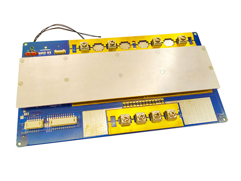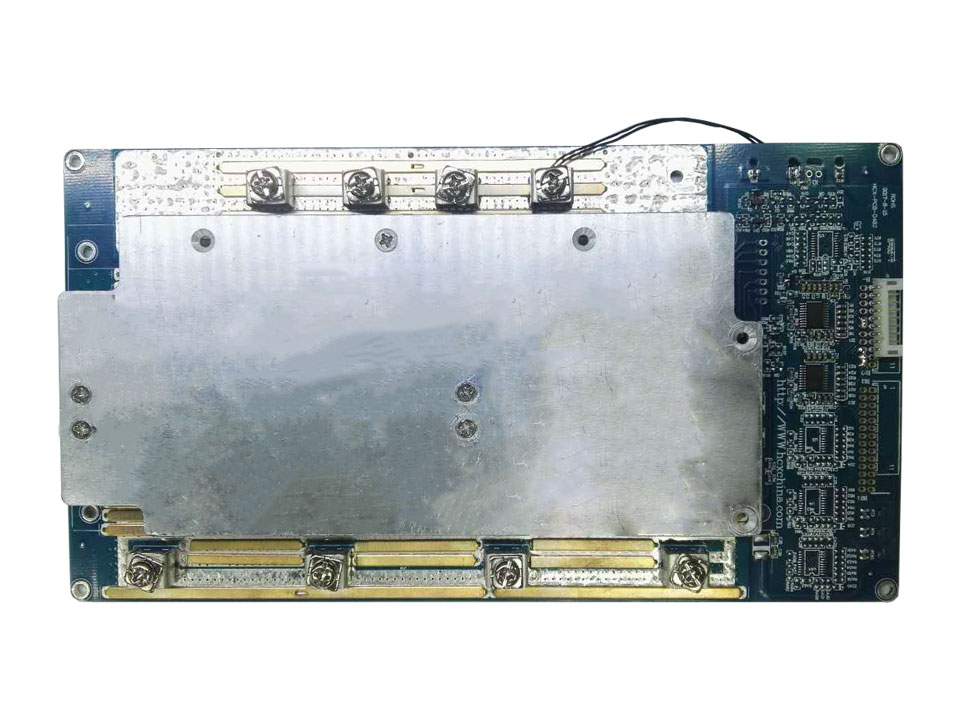
产品名称:3串70A同口带均衡三元锂电池保护板
规格型号:HCX-PCB-D482
物料编码:D482LI03S70A
产品描述:3串保护板充电70A放电70A带均衡
保护参数:
1.电压保护Voltage protection
2.电流保护Current protection
3.温度值Temperature thresholds
4.均衡
保护参数:
1.电压保护Voltage protection
| 项目ITEM: | 保护值Protection thresholds: | |
| 充电电压 | 12.6 | TBD |
| 过充电检测电压Over-charge detection voltage (per cell) | 4.250± 20mV (per cell) | V |
| 过充电延时间Over-charge detection delay time | 1 | S |
| 过充电恢复电压 Over-charge release voltage (per cell) | 4.150± 50mV (per cell) | V |
| 过放电检测电压Over-discharge detection voltage (per cell) | 2.70± 50mV (per cell) | V |
| 过放电延时间Over-discharge detection delay time | 1 | S |
| 过放恢复电压Over-discharge release voltage (per cell) | 2.90± 100mV (per cell) | V |
| 项目ITEM: | 保护值Protection thresholds: | |
| 硬件放电过流检测 1 | 150A ± 15A | A |
| 过电流1延时Over-current detection delay time 1 | 650-830 | ms |
| 过电流2检测电压Over-current detection2 | 300A ± 30A | A |
| 过电流2延时Over-current detection delay time 2 | 50-150 | ms |
| 短路保护SCD detection | >=600A | A |
| 负载短路检测延迟时间SCD delay time | 360 | uS |
| 电过/短路保护恢复 | 移除负载 恢复 |
| 项目ITEM: | 保护值Protection thresholds: |
| 充电高温温度保护OTC | 50℃ |
| 放电高温温度保护OTD | 70℃ |
| 充电低温温度保护UTC | 0℃ |
| 放电低温温度保护UTD | -20℃ |
| 均衡开启电压 | 4.2V±0.025V |
| 均衡电流 | 84±10 mA |
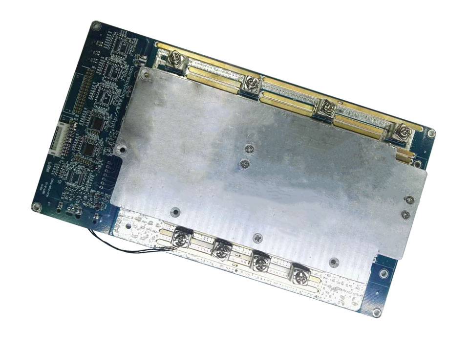
5.PCB尺寸图
")
PCB尺寸:220×120(高度28-32mm)
静态电流≦20μA
3串最大持续充放电电流70A
示意图 : 方框图
")
6.接口定义
7.主要元器件清单示意图 : 方框图
6.接口定义
| 接口 | 符号说明 |
| PACK-(P-) | 充电时接电源负极,放电时接负载负极.此接口为大电流接口,请根据负载电流选用合适规格的线材 |
| BATT-(B-) | 接电池负极.此接口为大电流接口请根据负载电流选用合适规格的线材 |
| 3.7V(B1) | 第1节电芯正极第2节电芯负极3.7V |
| 7.4V(B2) | 第2节电芯正极第3节电芯负极7.4V |
| 11.1V(B3) | 第3节电芯正极第4节电芯负极11.1V |
| ..... | ............. |
| B+ | |
| PACK+(P+)/B+ | 充电时接电源正极,放电时接负载正极.此接口为大电流接口,请根据负载电流选用合适规格的线材 |
| HCX-PCB-D482 | 24S/150A 220×120×1.6/FR-4 | PCS | 1 | PCB |
| HCX-PCB-D482B | 20串均衡板 34.5×120×1.6/FR-4 | PCS | 1 | PCB |
| IC-637 | BQ7790509/过充4.25V/过放2.5V/过流检测50mV/100mV | PCS | 1 | U1 |
| MOS-295 | MOSFET/HY4004P/40V/208A/2.5mR/N管/TO-220/HY | PCS | 16 |